
The way little silicon chips are running the world.
By Tanmay Goel/GuyPhy (consultant w/ Bluethroat Labs) originally published on BitCrusader
Bluethroat Labs publishes foundational content like this because TEE security requires understanding the stack TEEs are built on. This is that foundation.
Computers are everywhere. From the smartphone in your pocket to the supercomputers powering scientific breakthroughs, these machines have become an indispensable part of modern life (so much so that the smallest of software bugs can bring the world to a halt!). We use them to browse the web, play games, edit pictures, and even control entire stock exchanges. The device you are reading this article on is a computer. But what happens between the moment you do an action on your computer and the moment you see the result on your screen? Have you ever stopped to wonder: What and how does a ‘computer’ actually compute?
In this article, we’ll take a deep dive into how modern computers work on a fundamental level. We’ll start with the basics: what a computer is and what it’s meant to do. From there, we’ll explore how programs—consumed and written by users like you—are translated into a language the computer can understand. We’ll peel back the layers of abstraction to reveal the inner workings of the machine, from the low-level assembly language to the fundamental architecture that makes computation possible. Along the way, we’ll examine the key components involved, such as memory, processors, and input/output devices, and explain how they work together to execute instructions.
What is a Computer?
At its core, a computer is a device designed to compute—to process information and perform specific tasks based on a set of instructions. But this seemingly simple definition masks an intricate dance of hardware and software, a system of electrical signals and logical operations that transform human-readable code into meaningful output. So let’s define what a computer is in more technical terms.
A computer can be broadly divided into two categories—hardware and software. The hardware consists of tangible components like the CPU, Memory, Storage and, Input/Output devices, whereas the software is the instructions, programs and routines responsible for operating the hardware.
The word “computer” has its roots in the Latin word “computare” which means to calculate or to count. Historically, the term "computer" referred to a person who performed calculations or computations. After the creation of early mechanical computers in the mid-1800s and the invention of ENIAC (Electronic Numerical Integrator and Computer) in 1946, the word “computer” assumed its more modern meaning of “The Digital Programming Machine”. Early computers were purpose-built for very specific sets of calculations but modern computers are digital, programmable and capable of executing a wide range of tasks.
The term computer is not limited to just laptops or desktops; they include smartphones, tablets, servers, and even small embedded systems. We are surrounded by computers, be it your smart TV, the infotainment system in your car, checkout kiosk at the grocery store, etc. What ties each of these devices to the same term is their ability to execute instructions and process data.
What is Expected of a Computer?
For an everyday user, computers are tools to perform tasks efficiently and accurately. Some common applications of the computer are running applications (e.g., web browsers, games, text editors, productivity software), storing and retrieving data infallibly, connecting to other devices and the internet, etc.
Users also expect a computer to execute tasks quickly and efficiently without any errors. Any incorrect outputs, delays in execution, or crashes are seen as failures. A computer should provide high-level interfaces such as graphical user interfaces, screens, networking interfaces (e.g., Wifi, ethernet, Bluetooth, SIM) navigation interfaces (e.g., keyboards, mouse, controllers, touchscreens), and input interfaces (e.g., storage devices, other peripherals such as smart card readers, fingerprint scanners, serial ports) to provide users the ability to program and run applications easily.
A computer should not require most users to know how it works internally. While the users interact with the provided interfaces the computer is executing millions of instructions every second. This gap is bridged by several layers of abstraction from high-level programming languages to compilers and machine code.
To understand how a computer meets these expectations, we need to explore what it actually computes—starting with the concept of a program.
What Does a Computer Compute? (It’s a Program)
A computer program is an unambiguous and ordered set/sequence of instructions in an interpretable language for the computer to execute. A program is constructed by first using a description of logical and mathematical operations expressed in an appropriate human-readable programming language to execute a specific task. This description is then transliterated (in multiple stages) into the program which can then be directly executed on the computer. Programs are created to solve problems or automate tasks which can range from extremely simple (e.g., adding two numbers) to highly complex (e.g., simulating weather patterns). Programs also need data to operate on, which can be obtained from user input, retrieved from storage, or received from external sources such as sensors, and networks.
Before diving into the stages of a program and its execution, it’s helpful to understand a few key terms. Source code is the human-readable version of a program written by developers. Compiling is the process of turning this source code into binaries, which are machine-readable instructions. Linking combines these binaries with necessary libraries (which are just pre-written utility programs) to create an executable, a file ready to run. The operating system manages the program’s execution, loading it into memory (the computer’s temporary workspace) and starting it at the entry point, where the program begins running. These steps ensure the program works seamlessly with the computer’s hardware.
#include <stdio.h>

int main() {
    printf("Hello, World!\n");
    return 0;
}
‘Hello World’ program written in C, a high-level programming language.
When a program is created, it goes through several stages before it can run on a computer. First, the program is written in source code which is then compiled at compile time, where it is translated into machine-readable code. During this stage, the program may also be statically linked, meaning any necessary libraries are combined with the code to create an executable file. Once the executable is ready, the operating system takes over. At load time, the operating system loads the program into memory and may perform dynamic linking, connecting the program to additional libraries as needed. The program then enters run time, where execution begins at the program's entry point. The program runs until it either completes its tasks and terminates normally or encounters an error and crashes. Each of these stages relies on the Application Binary Interface (ABI) of the operating system, which defines how the program interacts with the computer's hardware. Together, these stages ensure that the program can be written, translated, loaded, and executed efficiently on the hardware.
All of this sounds complicated, what exactly is a program from the perspective of a user?
What is a Program from the Perspective of a User?
For most users, programs are “black boxes”. The users expect to provide input and receive correct output without needing to understand how programs are constructed and executed internally. For example, clicking on the ‘Save’ button in a text editor involves multiple layers of operations (e.g., interpreting the user intent to save the document, file system interactions, memory operations, etc.). Users don’t need to know about these operations but still expect their work to be saved. This attribute of computers is arguably the most important as it makes them accessible to non-technical users.
Programs are packaged as applications that abstract away the complexity of underlying computations from users. These applications (and by extension programs) are what we use every day to accomplish tasks such as writing documents, playing music, social media, browsing the web, writing other applications and so much more. Users interact with interfaces of these applications such as buttons, menus, windows, swipes, taps, or in some cases Command-Line Interfaces (CLIs) to provide inputs and the application computes on these inputs to provide desired output.
While applications provide interfaces to users at a high level, the computer needs to understand these programs at a much lower level, which brings us to the next step—how computers interpret and execute programs.
How Does the Computer Understand a Program? (Compilation into Assembly)
Applications and programs are written in high-level human-understandable languages such as Python, C++, or Java but computers can only understand binary code (1s and 0s). This creates a gap between how humans can provide instructions and how a computer can receive them. This language barrier needs to be bridged by a translation process. There are many ways this is done in modern computers, “compilation” being the generally used term for the translation process. The compilation is performed by another program called a “compiler”.
We are not differentiating between different types of translators i.e. assemblers, compilers, and interpreters for simplicity.
A compiler is a computer program that takes code in one language and translates it to another language. Most compilers are made to translate high-level programming languages into low-level assembly language or machine code thus creating a set of instructions that the computer can understand and execute. Compilers are very complicated pieces of software and the translation process contains multiple operations performed in “phases”.
First, the preprocessing phase prepares the program by handling directives like including libraries, expanding macros, language extensions, etc. The preprocessed code is then put through lexical analysis which breaks down code into smaller lexical tokens such as identifiers, data types, operators, keywords, literals, punctuators, whitespaces, etc. according to rules of the lexical grammar (lexical grammar serves the same purpose for a programming language as grammar does for natural language) for the programs’ high-level language. The tokens generated go through parsing next which builds a structural representation (often a hierarchal structure such as an abstract syntax tree) while checking for functionally correct syntax. This structured representation is then put through semantic analysis which adds semantic information to it, performs semantic checks (such as type checking, object binding, label checks, flow control checks, definite assignment, etc.), and constructs a symbol table. The symbol table is a data structure that contains information about the declaration and usage of each symbol in the source code. Semantic analysis ensures that the declarations and statements of the program are semantically correct, i.e., that their meaning is clear and consistent with the way in which control structures and data types are supposed to be used while flagging incorrect programs with warnings or errors. After this, the code is converted into an intermediate representation, a simplified version designed to represent source code without any loss of information while being independent of any target platform. The intermediate representation is then put through the code optimisation phase which improves the code’s efficiency. Finally, the code generation phase takes in the optimised intermediate representation and produces machine-specific instructions that the computer’s hardware can execute. This is called the object code. Object code is the compiler output for each file of the source code. The linker then takes all relevant object files for a source code and links them all together to create a single executable file, resolving any references to external functions or variables and managing symbol resolution and memory relocation.
These phases are often implemented as modular components, making the compiler efficient and reliable. Since errors in the compiler can lead to hard-to-find program faults, significant effort is put into ensuring the compiler works correctly, ensuring a smooth translation from source code to hardware execution.
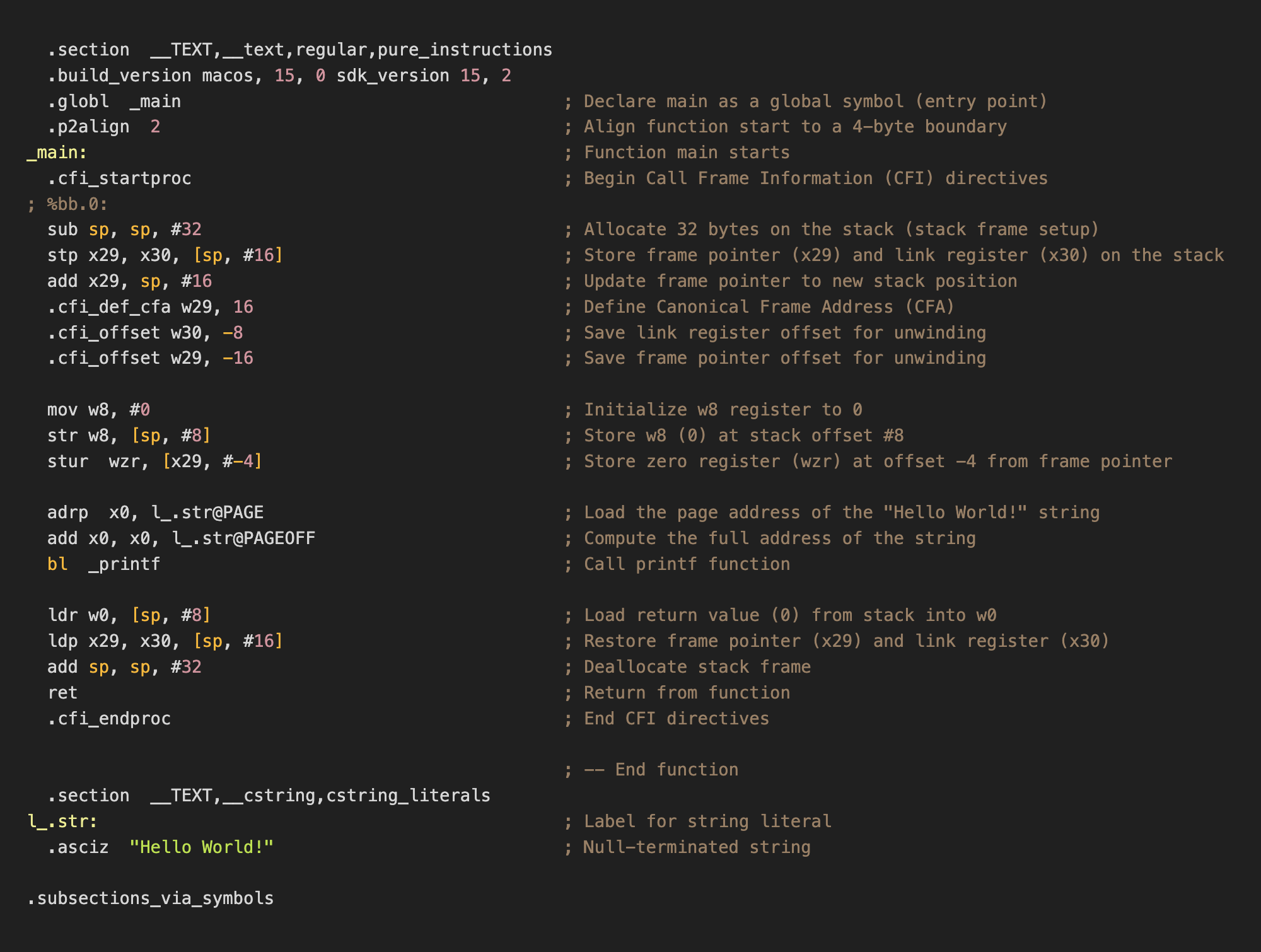
ARM64 Assembly translation of the ‘Hello World’ C program.1
After compilation, the source code is now converted into a set of platform-specific instructions or an assembly program.
What is Assembly?
Assembly language (simply referred to as assembly and abbreviated as ASM) is a low-level programming language consisting of instructions that can be directly converted into binary machine code (finally we are at 0s and 1s of a computer!) on the specific hardware architecture associated with the language. Assembly languages generally have a 1:1 mapping between their instructions and machine instructions but similar to high-level programming languages allow programmers to use features like constants, labels, loops, macros, directives, and comments to construct the program in a human-readable form (albeit with a lot more difficulty). Although the majority of general-purpose computers can perform almost identical tasks, they do them in different methods, which are reflected in the respective assembly languages.
Assembly languages use mnemonics—known as opcodes—to symbolically represent machine code instructions in a human-readable format. Each opcode can consist of zero or more operands. Operands can be either immediate (direct values), registers (smallest and fastest storage on a processor), or referred (external memory addresses) and represent input data, arguments, or parameters to the opcode. Opcodes define exactly what an instruction does and are often extremely simple such as moving a value from one location to another, adding two numbers or jump to a memory location (represented respectively by MOV, ADD, and JMP). In assembly opcodes can also be extended into microcode which can define more complex instructions, for which dedicated machine instructions are not available, using a combination of basic opcodes.
A very important distinction between assembly and high-level programming languages is that assembly code can unambiguously be translated directly into machine code and vice-versa with no interpretation required. This is fundamentally different from the compilation of high-level languages where changes in compiler logic can produce different object code but with the same functionality.
hello:	file format mach-o arm64

Disassembly of section __TEXT,__text:

0000000100003f58 <_main>:
100003f58: d10083ff    	sub	sp, sp, #0x20
100003f5c: a9017bfd    	stp	x29, x30, [sp, #0x10]
100003f60: 910043fd    	add	x29, sp, #0x10
100003f64: 52800008    	mov	w8, #0x0                ; =0
100003f68: b9000be8    	str	w8, [sp, #0x8]
100003f6c: b81fc3bf    	stur	wzr, [x29, #-0x4]
100003f70: 90000000    	adrp	x0, 0x100003000 <_printf+0x100003000>
100003f74: 913e6000    	add	x0, x0, #0xf98
100003f78: 94000005    	bl	0x100003f8c <_printf+0x100003f8c>
100003f7c: b9400be0    	ldr	w0, [sp, #0x8]
100003f80: a9417bfd    	ldp	x29, x30, [sp, #0x10]
100003f84: 910083ff    	add	sp, sp, #0x20
100003f88: d65f03c0    	ret

Disassembly of section __TEXT,__stubs:

0000000100003f8c <__stubs>:
100003f8c: b0000010    	adrp	x16, 0x100004000 <_printf+0x100004000>
100003f90: f9400210    	ldr	x16, [x16]
100003f94: d61f0200    	br	x16
Byte-Code disassembly representation of ‘Hello World’ C program.2
Since there is a 1:1 mapping of assembly instructions to machine code instructions, each assembly language is unique to a specific Instruction Set Architecture. The rules that specify how software communicates with a computer's central processing unit (CPU) are known as an Instruction Set Architecture (ISA). An ISA outlines the behavior of machine instructions of implementations of that ISA but does so in a manner that is independent of the specifics of said implementation. By serving as a link between hardware and software, ISAs make it possible for machine code created for one CPU to execute on another CPU with the same ISA, even in cases when the hardware designs are different. The ability to run software on faster, newer processors without requiring rewriting is known as binary compatibility. This makes ISAs one of the most fundamental forms of abstraction in computing.
00000000: 00000000 00000000 00000000 00000001 00000000 00000000  ......
00000006: 00111111 01011000 11010001 00000000 10000011 11111111  ?X....
0000000c: 10101001 00000001 01111011 11111101 10010001 00000000  ..{...
00000012: 01000011 11111101 01010010 10000000 00000000 00001000  C.R...
00000018: 00000000 00000000 00000000 00000001 00000000 00000000  ......
0000001e: 00111111 01101000 10111001 00000000 00001011 11101000  ?h....
00000024: 10111000 00011111 11000011 10111111 10010000 00000000  ......
0000002a: 00000000 00000000 10010001 00111110 01100000 00000000  ...>`.
00000030: 00000000 00000000 00000000 00000001 00000000 00000000  ......
00000036: 00111111 01111000 10010100 00000000 00000000 00000101  ?x....
0000003c: 10111001 01000000 00001011 11100000 10101001 01000001  .@...A
00000042: 01111011 11111101 10010001 00000000 10000011 11111111  {.....
00000048: 00000000 00000000 00000000 00000001 00000000 00000000  ......
0000004e: 00111111 10001000 11010110 01011111 00000011 11000000  ?.._..
Binary executable of ‘main’ function of ‘Hello World’ C program.3
ISAs are categorised according to their level of complexity; RISC (Reduced Instruction Set Computer) concentrates on simpler, more commonly used instructions for increased efficiency (e.g. ARM, RISC-V, etc.), while CISC (Complex Instruction Set Computer) offers a wide variety of specialised instructions (e.g., Intel x86, PDP-11, etc.). Other varieties, such as VLIW (Very Long Instruction Word), are designed to increase performance by delegating complicated tasks to the compiler and executing multiple instructions in parallel (e.g., Intel Itanium IA-64, Elbrus 2000, TeraScale, etc.).
Assembly programs are linked and then translated into binary machine code using an assembler which decodes opcode mnemonics and resolves addresses. Now we have the binary input on which the computer can compute, but how exactly does the computer hardware understand these binaries? Let’s understand the hardware side of a computer that can speak and understand the language of 1s and 0s.
How to Build a Computer? (The von Neumann Architecture)
The term architecture (in the context of computer processors) refers to specifications defining the design and implementation of the “Central Processing Unit” (CPU) or “Processor” of a computer. The CPU is responsible for executing program instructions. A particular digital processor implements a specific instruction set architecture (ISA), which specifies the set of instructions and their binary encoding, the set of CPU registers, and the implications of executing instructions on the processor's state. As long as the ISA definition is adhered to, different microarchitectures can implement the same ISA. For instance, AMD and Intel create distinct x86_64 ISA CPU implementations.
Regardless of the ISA, almost all modern processors follow the von Neumann Architecture Model (sometimes also referred to as the Princeton Model). The general-purpose design of the von Neumann Model enables it to run any kind of software. It employs a stored-program model, which means that both the program data and the program instructions are inputs to the processor and are stored in computer memory. It was first presented by John von Neumann in 1945 in his paper titled “First Draft of a Report on the EDVAC”. The EVDAC (Electronic Discrete Variable Automatic Computer) was the successor to ENIAC with the primary differentiators being that the EVDAC was a binary computer instead of decimal, and it was a stored-program computer. This model has been the blueprint for virtually all computers since its conception.
The first computers were re-configurable for a certain purpose rather than being “programmable" for it. When feasible, "reprogramming" was a time-consuming procedure that began with paper notes and flowcharts, progressed to detailed engineering drawings, and ended with the difficult task of physically rewiring and rebuilding the machine. On the ENIAC, setting up and debugging a program could take up to three weeks! A computer's ability to store data and instructions in the same memory is the foundation of the von Neumann architecture. The stored-program concept allows computers to be flexible and programmable. Instead of being hardwired to perform specific tasks, a computer can load different programs into memory and execute them as needed. This is why a laptop can switch from browsing the web to editing a video with just a few clicks.
The von Neumann Architecture is made up of four main components:
-
Central Processing Unit (CPU) The CPU is referred to as the ‘brain’ of the computer. It is responsible for the execution of instructions of a program. The CPU is divided into two parts:
-
Control Unit (CU) The Control Unit drives the execution of program instructions by loading program instructions from memory and supplying the processing unit with instruction operands and operations. In order to track the state of execution and next instruction to schedule, the control unit also has some storage. The Instruction Register (IR) holds the instruction that is currently being executed, which is loaded from memory, and the Program Counter (PC) stores the memory address of the next instruction to execute. It also instructs the computer's memory, arithmetic and logic units, as well as its input and output devices, on how to respond to commands supplied to the processor.
-
Arithmetic / Logical Unit (ALU) The ALU consists of the circuitry that performs mathematical operations (e.g., addition, subtraction) and logical operations (e.g., comparisons). It also contains a set of registers. Registers are small but extremely fast storage units used to hold program data, instruction operands, and execution results from the ALU.
-
-
Memory The concept of internal memory is an indispensable innovation of von Neumann architecture enabling fast data storage near the processor and reducing calculation time. It holds both program data and instructions, forming the basis of the stored-program model. Memory size varies by system, but its addressable range is limited by the system’s ISA. The term “memory” can refer to different storage levels, including processor registers and secondary storage like HDDs or SSDs. However, in this context, ‘memory’ specifically refers to internal Random Access Memory (RAM) which allows direct access to all storage locations and can be visualised as a linear array of addresses.
-
Input / Output Devices Input and Output devices (often referred to in shorthand as I/O Devices) allow a computer to interact with the outside world. Input devices (e.g., keyboard, mouse) feed data into the computer, whereas output devices (e.g., monitor, printer) display or communicate computing results.
-
System Bus Although the System Bus is not considered a fundamental part of the original von Neumann Model, it has evolved into a necessary component to provide modularity and scalability to the model. The System Bus can be described as a single communication pathway linking all key hardware components of a computer, functioning as a digital backplane. It integrates three key functions: the data bus, which transfers information; the address bus, which specifies where data should be read from or written to; and the control bus, which manages operations and signal coordination.
The von Neumann Model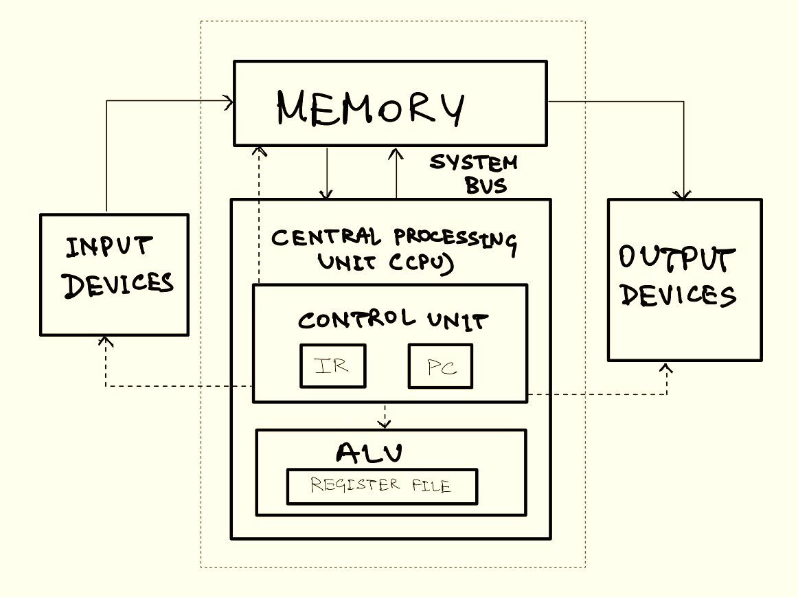
The von Neumann architecture is revolutionary because of its simplicity and versatility. By storing both instructions and data in the same memory, computers can be reprogrammed for new tasks without requiring physical changes to the hardware. This adaptability is what distinguishes computers as general-purpose machines, capable of operating everything from basic calculators to powerful artificial intelligence models. However—as the early computers started scaling up in performance and efficiency while scaling down in size—a major limitation of the model was realised, the von Neumann Bottleneck.
The von Neumann bottleneck is a constraint in classic von Neumann architecture induced by a shared communication line between the CPU and memory. Because both data and instructions pass through the same system bus, the CPU frequently has to wait for data to be sent, which slows overall performance especially when handling large data sets with minimal computation. This causes a bottleneck, limiting the rate at which a system can process information. As CPU speeds and memory sizes have grown much faster than bus throughput, this bottleneck has worsened, becoming more problematic with each new CPU generation. In 1977, John Warner Backus critiqued the von Neumann Model during his ACM Turing Award lecture:
Surely there must be a less primitive way of making big changes in the store than by pushing vast numbers of words back and forth through the von Neumann bottleneck. Not only is this tube a literal bottleneck for the data traffic of a problem, but, more importantly, it is an intellectual bottleneck that has kept us tied to word-at-a-time thinking instead of encouraging us to think in terms of the larger conceptual units of the task at hand. Thus programming is basically planning and detailing the enormous traffic of words through the von Neumann bottleneck, and much of that traffic concerns not significant data itself, but where to find it. [Reference]
- Words are the smallest addressable units of memory in a given architecture.
Over the decades, engineers have been continuously finding ways to work around this limitation and push the boundary of performance. In fact, much of the complexity in modern processor design and architecture can be attributed to mitigation efforts of the von Neumann bottleneck. Let’s look at some of these mitigations and understand what exactly makes a computer modern.
The Modern Computer
The Von Neumann architecture laid the foundation for modern computing, but today’s processors are far more advanced than their predecessors. High-level programming languages allow programmers to think about the broader task-at-hand with paradigms like functional programming and object-oriented programming, abstracting the memory management complexities of early programming languages, and mitigating some effects of the intellectual bottleneck mentioned by Backus. Nevertheless, the underlying architectures—even today—are "pushing vast numbers of words back and forth".
In this section, we’ll first look at some key components that form the building blocks of a physical processor, understand how these building blocks are arranged together to make a functional processor and then dive deeper into the architectural concepts that make modern processors so powerful despite previously mentioned limitations.
What is a processor made of? The Staples
Contemporary processors are complex pieces of hardware, capable of executing billions of instructions every second! To understand how these processors are built we need to start with the basic building blocks of digital design. These components—though simple in isolation—come together to form the intricate machinery that powers modern computing.
-
Logic Gates
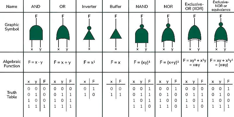
Logic gates are the building blocks of the circuitry that makes up any digital binary computer. The design of complicated digital circuits is achieved through multiple layers of abstraction. Simple circuits are designed using logic gates for basic functionality, these simple circuits are abstracted from their implementation and used as building blocks for creating more complicated circuits. These circuits can be further abstracted to create more complicated circuits. The process is continued until the designers have complete circuits for the functional components of a computer. Logic gates are constructed from **transistors** placed on semiconductor materials like silicon wafers. Transistors act as switches, controlling electrical flow. They switch between on and off (high or low voltage) based on their input and current state. These voltages represent binary values: high (1) and low (0). On the lowest abstraction, all circuits are built from logic gates connected together to perform boolean operations. A logic gate takes one or two binary inputs and produces a binary output based on a logical operation. There are several different types of logic gates created using either transistors or other logic gates. The AND, OR, and NOT gates (corresponding to conjunction, disjunction, and negation operations respectively) are considered an elementary set of gates, through which any other circuits can be constructed. In Boolean algebra, minimal sets are those that contain the fewest number of operators necessary to express all Boolean functions. One such example is the NAND gate, which is a universal logic gate as it has functional completeness property. This means that an entire processor can be implemented using only NAND gates! In fact (due to simplicity, efficiency amongst other reasons) general purpose processors are almost exclusively made using only NAND gates.
-
Circuits
Now that we understand how logic gates work, let's look at some of the circuits which implement the core functionalities of an ISA. A circuit is formed by connecting sub-circuits and logic gates. Primitive circuits of a processor can be broadly classified into three categories:
-
Arithmetic / Logic Circuits: These circuits are responsible for executing logical and arithmetic operations on the processor. These operations can include adding two numbers, comparing two numbers, shifting bits left or right for a binary number, etc.
-
Control Circuits: These circuits control the execution of program instructions on program data. They regulate the loading and storing of values to various levels of memory, as well as the operation of system hardware components. Multiplexers (MUX) and Demultiplexers (DMUX) are examples of control circuits. A MUX selects one input from multiple signals and forwards it to a single output while a DMUX takes a single input and distributes it to one of several outputs.
-
Storage Circuits: These circuits provide the necessary storage for binary numbers on a computer. Storage circuits are primarily of two types, Static Random Access Memory (SRAM) and Dynamic Random Access Memory (DRAM). SRAM is built using circuit-based storage, is the most stable and fastest memory on a processor (albeit being the most expensive), and is used in CPU registers and on-chip cache memory. In contrast, DRAM is slower but orders of magnitude cheaper. It uses grids of capacitors to store data, with a charged capacitor representing logical 1 and no charge representing logical 0. Since capacitors leak charge gradually, DRAM needs periodic refreshes to keep its data intact. A typical SRAM cell is made up of 6 transistors (known as a 6T SRAM Cell) and can store 1 bit of information.
Another important storage circuit is a flip-flop. Flip-flops are clocked sequential circuits that store a single bit of data and are commonly used in process registers, buffers, etc (when combined to create multi-bit storage). Since flip-flops are inefficient in terms of power and area requirements compared to SRAM cells, they are only preferred in ultra-fast, small-bit storage applications.
- Clock Circuits - Most modern CPUs operate as synchronous circuits, which means they rely on a clock signal to regulate their sequential operations. The clock signal, generated by an external oscillator, produces a consistent square wave of pulses that determine the speed at which the CPU executes the instructions - the higher the frequency (typically measured in hertz, or cycles per second), the faster the execution. For all processor components to function correctly, the clock duration should be longer than the longest signal propagation time within the CPU. By setting the clock higher than the worst-case propagation delay, designers can simplify CPU architecture and ensure synchronised reliable data movements along the edges of the clock. However, this approach also means that the fastest components now wait for slower components, limiting overall performance. To reduce this effect, modern CPUs employ techniques to increase equality, allowing different parts of the processor to work together and improve overall efficiency.
-
The parts of a processor—logic gates, circuits, and clocks—are organised in a structured form into specialised units that communicate to process instructions. At the heart of this structure is the ALU, which actually executes instructions received from programs. The ALU is supplied with inputs from the Register File, a small but very fast storage unit that holds data and instructions under processing. The Register File typically comprises general-purpose registers used for the storage of temporary data, as well as special-purpose registers like the Program Counter, Instruction Register, Status Register, Constant Registers, etc. The Control Unit manages data and instruction transfer between the ALU, registers, and memory. It decodes instructions read from memory, determines the operations required, and sends control signals to the desired units. For example, if an instruction requires the addition of two numbers, the CU will tell the ALU to read the operands from the Register File, execute the ADD opcode, and write the result to a register. The CU also manages the clock signal, allowing all operations to be synchronised and performed in the right order. Data and instructions travel through different architectural units through buses, which are paths for the transfer of information. In cases where larger amounts of data are too big for the Register File to hold, the processor utilises cache memory and RAM (also referred to as “Main Memory”). This intricate arrangement—including the ALU, registers, control unit, buses, and memory—makes up the primary structure of a processor's operation. Now that we understand the building blocks of a processor and how they are arranged, let’s look at how these components work together to do computation.
What Does a Processor Do? (The Execution Pipeline)
At its heart, every processor has a mechanism to execute instructions called the Execution Pipeline. There are multiple ways to construct an execution pipeline with our arsenal of building blocks, the most fundamental one being the 5-Stage RISC Pipeline. As the name suggests, the 5-stage RISC pipeline divides the execution flow into 5 different stages—namely, Fetch-Decode-Execute-Memory-WriteBack. To enable instructions to execute in different stages, the processor uses special pipeline registers to act as intermediate buffers for the instruction. Each stage in the pipeline generally takes one clock cycle to execute (also known as the “latency” of that stage).
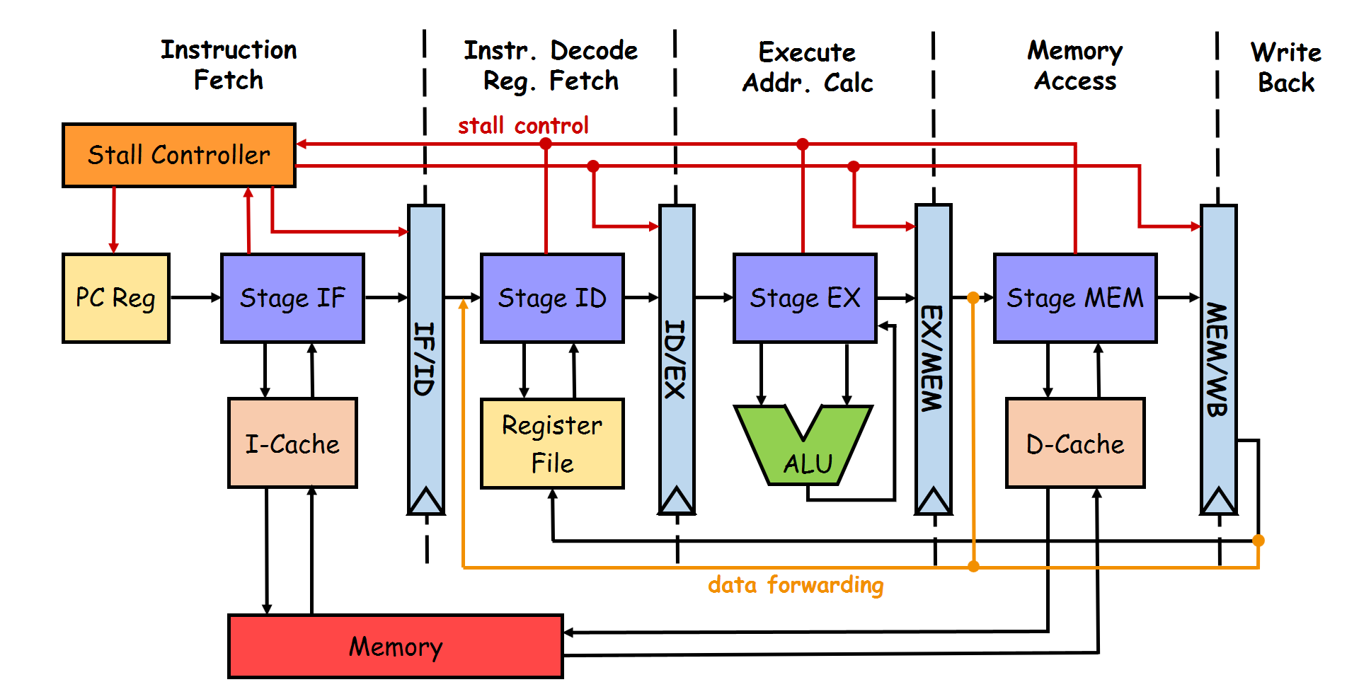
The above image shows the schematic diagram of a 5-stage RISC pipeline. Let’s unwrap each component:
Instruction Fetch (IF) Stage
The IF stage is responsible for fetching the instruction to be executed from the a small and extremely fast memory space known as the Instruction Cache. The Program Counter (PC) provides the address of the instruction to be fetched. Once fetched the instruction is stored in a special register known as Instruction Register (IR), and the PC is updated simultaneously updated to point to the next instruction to be executed.
Instruction Decode (ID) Stage
As we’ve already discussed, each instruction in a program contains an “opcode” which encodes what that particular instruction is supposed to do. In the ID stage, the opcode for the instruction in execution is decoded to determine what operation needs to be performed by the ALU. The processor identifies the opcode (such as ADD, JMP, LOAD, etc.) and also extracts the “operands” (which can be data or memory addresses needed to execute the instruction). The decode stage also reads data from the “Register File” (if needed). The instruction format can be generalised to OPCODE | SOURCE1 | SOURCE2 | DESTINATION. Here, Source 1 and Source 2 represent the operands on which the computation is to be done and the Destination is where the computed result is to be stored. The decoded opcode along with all the required operands is then passed onto the next stage.
Execute (EX) Stage
We’re here! This is where the computer computes. The EX stage contains the ALU which houses the circuits to perform arithmetic and boolean operations. A simple ALU has the capability to perform addition, division, bit-shifts, and boolean logic (such as AND, XOR, etc.) along with the functionality of providing status bits and flags for computation performed. These are helpful for indicating the state of the result to other processor components without needing to transfer the entire result (e.g., result is zero, overflow, NaN, etc.).
A control signal (from the ID stage) is provided to the MUX controlling the ALU to indicate which computation circuits need to be used and which registers to use as operands. For a simple RISC processor, the class of instructions executed can be broadly divided into three categories based on the “latency” of execution:
-
Register-Register Operations (one cycle latency): Direct instructions such as addition, compare, and logical operations are called Register-Register operations as the operands are used from and written to the “Register File” directly. During the execute stage the operands are fed to the ALU directly from the Register File and by the end of the clock cycle, the results are generated.
-
Memory Reference (two-cycle latency): Memory reference instructions (such as the
LOADandSTRinstructions) fall under this category. During the execute stage, the ALU takes in the base address from a register, and an offset is provided as an operand to compute the address of the new memory location to be accessed. After the reference address is computed the contents of that memory location are referenced. An example from our “Hello World” program isstr w8, [sp, #8]. Here the instruction is to store value in registerw8to the address which at an offset of8to the address insp. -
Multi Cycle Operations (multiple cycles of latency): Instructions in this category are more complicated to compute, such as division, multiply, and non-integer (or floating-point) operations. The ALU has special circuitry to execute these instructions. To free up the rest of the pipeline for execution, multi-cycle operations use a subset of the Register File.
Memory Access (MEM) Stage
If any instructions need to access memory other than the Instruction Cache or the Register File (generally it’s the Data Cache), it is done in the MEM stage. Instructions such as LOAD and STR access the memory address computed in the EX stage. Arithmetic or logical instructions that do not involve memory are simply marked as NOP (no-operation) for the MEM stage and forwarded to the next stage. This ensures both one and two-cycle latency instructions write their results to the Register File in the same stage, reducing complexity.
WriteBack (WB) Stage
The WB stage writes the result of the instruction back to the appropriate register in the Register File. For memory operations, the result might be written to a register after being fetched from memory. Once the instruction is done with the WB stage, it is considered executed. The Register File contains separate access points—called “ports”—for read and write operations. The ID stage reads the registers to provide operands to the EX stage while the WB stage simultaneously writes the results to an instruction’s target register.
The 5 Stage RISC Pipeline is the most fundamental model for creating an execution flow for a processor. One of the most important features of the execution flow is right there in the name— “pipeline”. The term pipeline is used because just like how a real-world pipeline allows water to flow continuously rather than one drop at a time, the execution pipeline overlaps different instructions moving at the same time, allowing simultaneous execution and making it much faster and more efficient (the alternative is waiting for an instruction to finish execution entirely before starting the next one, significantly reducing throughput).
Here’s a simplified example of how the pipeline works for five instructions:
As you can see, by the fifth cycle, the processor is actively working on all five instructions at different stages of the pipeline. An ideal pipelined processor executes one instruction every cycle to achieve the maximum possible throughput. The formal terminology for this is CPI (Clock cycle Per Instruction), with the ideal processor having a CPI of 1 (we’re going to see why a processor with CPI 1 is not achievable in practice). Pipelining exploits Instruction Level Parallelism (ILP), which is a notion in computer architecture in which many instructions are performed concurrently within a single CPU core, taking advantage of the inherent parallelism in a program's instruction stream. Let’s understand this better with an example:
| Cycle | Instruction 1 | Instruction 2 | Instruction 3 | Instruction 4 | Instruction 5 |
|---|---|---|---|---|---|
| 1 | Fetch | - | - | - | - |
| 2 | Decode | Fetch | - | - | - |
| 3 | Execute | Decode | Fetch | - | - |
| 4 | Memory | Execute | Decode | Fetch | - |
| 5 | Writeback | Memory | Execute | Decode | Fetch |
| 6 | - | Writeback | Memory | Execute | Decode |
| 7 | - | - | Writeback | Memory | Execute |
Consider the following series of arithmetic operations
A = B + C       - Instruction1
D = A * 3       - Instruction2
E = X OR Y      - Instruction3
Instruction 2’s result depends on the result of instruction 1 (because D cannot be computed without calculating A in the first instruction) but instruction 3 is completely independent of the previous instruction. This means that the execution of instruction 3 can be simultaneously and independently calculated with instructions 1 and 2. This means that if each instruction executes in one unit of time, all 3 instructions can be executed in two units of time—giving the program an ILP value of 3/2. Modern processors and compilers spend considerable resources to extract as much ILP benefit as possible.
Pipelining of execution flow is a cornerstone of processor design but—as with all good things—it does not come without its own challenges. Programmers generally write programs with the assumption that the execution of the program is going to be sequential, i.e., each instruction is completed before the next one begins. But as we already demonstrated, this is an abstraction provided by the processor, and under the hood, instructions execute in parallel and some instructions might finish execution before previous instructions in the sequence have been completed. If this abstraction is not fool-proof, it can create unexpected behavior in programs and even incorrect execution (such as value of D being incorrect in the above example). Execution orders in which instructions produce incorrect answers are known as Hazards. We’ve already introduced the possibility of a hazard on our execution flow (see if you can spot it before reading ahead!).
The Register File is simultaneously read from by the ID stage and written to by the WB stage. In the above example, if instructions 1 and 2 are scheduled sequentially onto the pipeline when instruction 1 is in the EX stage, instruction 2 is at the ID stage. Since instruction 2 takes the result of instruction 1 (i.e. A), the ID stage is going to provide it as an operand to instruction 2. The problem here is that the value of A given to instruction 2 is incorrect as the computed value is not going to be available in the Register File for another two cycles and hence the value of D is going to be incorrect.
There are mainly three types of hazards for a pipelined processor:
-
Structural Hazards
-
These occur when two instructions are looking to utilise the same resource on a processor at the same time. For example, two instructions require access to memory in the same clock cycle or ID, and WB requiring access to the Register File.
-
The usual solution to mitigate structural hazards is to add hardware for resources that are under contention. Examples include introducing separate instruction and data caches for the pipeline or providing multiple read and write ports to the Register File.
-
-
Data Hazards
-
Data hazards take place when an instruction—scheduled blindly—attempts to access data before its desired value is available. The example discussed above is categorised as a data hazard. There are three types of data hazards:
-
Read-After-Write Hazards (True-dependency hazards) - In a sequence of instructions, let’s say an instruction writes its results in register
R1, and the next immediate instruction reads from the same registerR1. The true value for the latter instruction should be the value computed by the former instruction, even before Writeback happens. -
Write-After-Write Hazards (Output-dependency hazards) - In a sequence of instructions, let’s say an instruction writes its results in register
R1, and the next immediate instruction also writes its result to the same registerR1. Any subsequent instruction in the pipeline should consider the value written by the latter instruction in registerR1as the true value, even before Writeback happens. -
Write-After-Read Hazards (Anti-dependency hazards) - In a sequence of instructions, let’s say an instruction reads the value of register
R1and the next immediate instruction writes to the same registerR1. The true value for the first instruction should be the original value inR1before the write operation occurs. If the write operation completes before the read operation (which can happen if the initial instruction is a multi-cycle instruction or has data dependencies on other incomplete instructions), the first instruction will incorrectly use the newly written value instead of the original one.
-
-
There are generally two ways to deal with data hazards in a RISC pipeline, operand forwarding and pipeline bubbles.
-
Operand Forwarding (also known as data forwarding or bypassing) is the process of passing the computation results as soon as they are available instead of waiting for the instruction to reach the WB stage. In the data hazard example discussed earlier, instruction 1 (
ADD) computes the value ofAin the EX stage while instruction 2 (MUL) is in the ID stage. In the next clock cycle, the true value ofAhas been computed but it cannot be used by instruction 2, unless the computed value of A is immediately forwarded to the EX stage, bypassing the WB stage. This means that instruction 2 can now be executed correctly. -
Pipeline Bubbles (also known as NOPs or Stalls) are special instructions to deal with data hazards by introducing a bubble in the pipeline, which results in the processor doing nothing for one cycle. In the previous example, if data forwarding is not available, the way to ensure correct execution would be to introduce two bubbles between instruction 1 and 2 so that when instruction 2 needs to compute using
Aas an operand, instruction 1 is at the WB stage and true value ofAis written to the Register File. The term bubble is used for no-operation instruction because just like in a water pipe where bubbles take up resources in the pipeline but do not contribute to the overall flow of water coming out of the pipe, NOPs do not contribute to the throughput of the processor. The stall controller (also referred to as pipeline interlock) is responsible for introducing bubbles where needed in the pipeline.
-
-
In practice, operand forwarding and NOPs are used in conjunction to mitigate data hazards.
It is because of NOPs that a real-world processor cannot achieve a CPI (Clock cycles per Instruction) value of 1. Since there are always going to be some fraction of total execution cycles spent as NOPs, the CPI for actual processors is always greater than 1.
\(CPI_{true} = CPI_{ideal} + Stall Cycles PerInstruction\)
-
-
Control Hazards
-
Control hazards are caused by either conditional or unconditional branching in a program (e.g., instructions like
JMP,BNE, etc.). Branches are instructions that alter the flow of execution based on certain conditions. They enable programs to make decisions and perform repetitive tasks by jumping to different parts of the code. Common examples include conditional branches (e.g.,if-elsestatements) and unconditional branches (e.g.,gotoor function calls). Branches are critical for implementing loops, error handling, and decision-making logic but they create inherent uncertainty in program execution. When the control of a program reaches a jump/branch instruction, the processor has to make a decision on whether to take the branch or not. Taking the branch means that the PC register is updated to point to the branch target address and not taking the branch means that the PC is incremented to point to the next sequential instruction as normal. When the jump/branch instruction reaches the EX stage, the processor figures out if the decision taken for the branch was correct or not. Depending on whether the branch is taken or not, the branch address (the address to which the CPU should branch out) is determined. If the earlier decision was incorrect, all instructions in the pipeline that had been fetched and decoded up to that clock cycle should be discarded. Because those instructions should not have been executed at all! This means flushing each stage of the pipeline with NOPs and fetching the instruction at the branch address in the following clock cycle. This incurs a significant number of clock cycles as a penalty. This is known as the "branch penalty." -
Control hazards can be mitigated by simply stalling the pipeline by inserting NOPs when a jump/branch instruction is encountered in the IF stage. The branch result can be computed in the EX stage and the PC can be updated to point to the next correct instruction (whether branch taken or not). The correct instruction is then fetched and pipeline execution resumes as normal. Although this approach might seem like a straightforward way to completely eliminate control hazards, in practice this is not practical. The frequency of branching logic in high-level programs combined with (at least) three stalls per jump/branch instruction means that simply introducing NOPs significantly reduces processor throughput. Let’s assume that 25% of instructions in a program are branch instructions and each branch instruction introduces three stalls. CPI for this program’s execution would be
\(CPI_{true} = (CPI_{ideal}*0.75)+(3*0.25) = 1.5\)
This is a 33% decrease in the processor throughput! Modern processors use a “branch predictor” in the IF stage to mitigate control hazards. In essence, the branch predictor (based on some pre-configured heuristics) guesses if a branch would be taken or not. If it guesses right, the execution resumes without any bubbles but if it guesses wrong the branch penalty is incurred and the correct execution flow has to be restored. This approach does not completely get rid of control hazards, but a good branch predictor can significantly improve performance of the processor. Let’s assume the same program, 25% of instructions being branch instructions with a three-cycle stall penalty, but with a branch predictor that predicts correctly 90% of the time. The
CPIis 1.05 in this case, reducing the throughput penalty from 33% to less than 5%!
-
We’ve now covered all components of the 5-Stage RISC pipeline from our diagram and how these components come to work together to create the execution flow that computes the programs we write. The entire execution pipeline (and to some extent, the entire processor) can be visualised as a giant “finite-state machine”. A state machine is a mathematical abstraction used to design systems consisting of a finite number of states, that read a set of inputs and transition to a different state based on those inputs. Each stage of the pipeline—fetch, decode, execute, memory, and writeback—can be thought of as a distinct state, with transitions occurring as instructions move through the pipeline. The diagram below shows the FSM for the execution flow discussed, illustrating how the processor transitions between states to process instructions efficiently.
Finite-State Machine Diagram for 5 Stage RISC Pipeline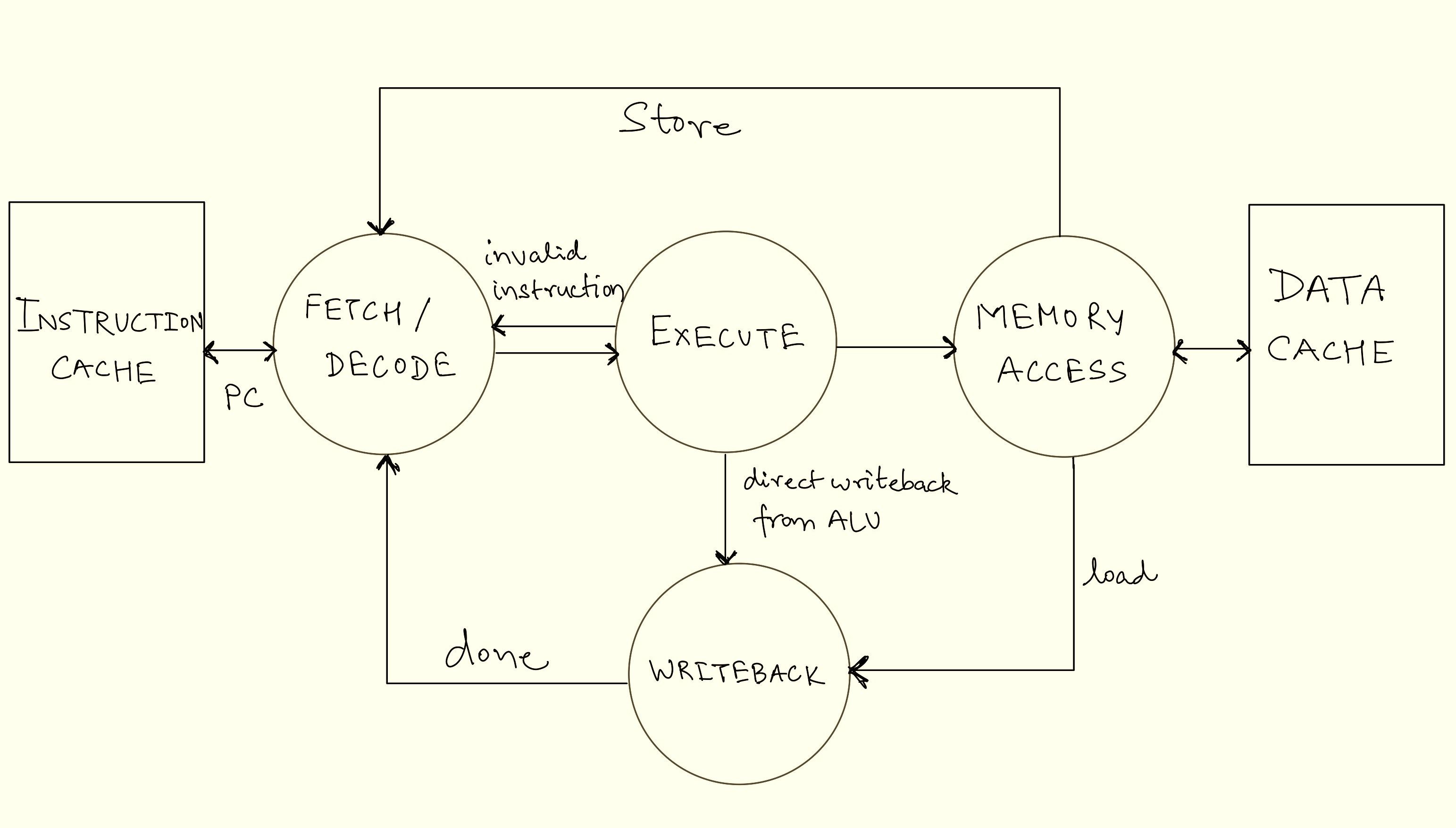
Using this execution flow, processors can compute large amounts of data very quickly. Assuming the rest of the processor can scale up as well, this simple execution flow can scale linearly with clock speeds. Meaning that with this simple design, a 1GHz clock signal would allow the processor to execute 1 billion instructions per second (it’s obviously not as simple in real processors though with limitations such as heat dissipation, transistor size, and inefficiencies in the execution flow like data hazards).
Although pipelining a processor comes with significantly increased hardware requirements and complexity, it remains a ubiquitous practice in all modern processor design. We’ve barely scratched the surface of how complex processor design is and how all the components of software and hardware come together to run any imaginable application. Let’s look at a few of the many architectural innovations that enable the processor to scale up to fulfil the computation needs of present-day applications.
Beyond the Basics: Scaling Processor Performance
While the 5 Stage RISC pipeline lays the foundation of a processors execution flow, modern processors face ever growing demands for performance and efficiency. Computer architects are constantly pushing the boundaries of the capabilities of a processor. In this section we’ll explore some key architectural innovations of advanced processor design which helps overcome the bottlenecks previously discussed and make them faster and more efficient.
Parallelism: Doing Many Things at Once
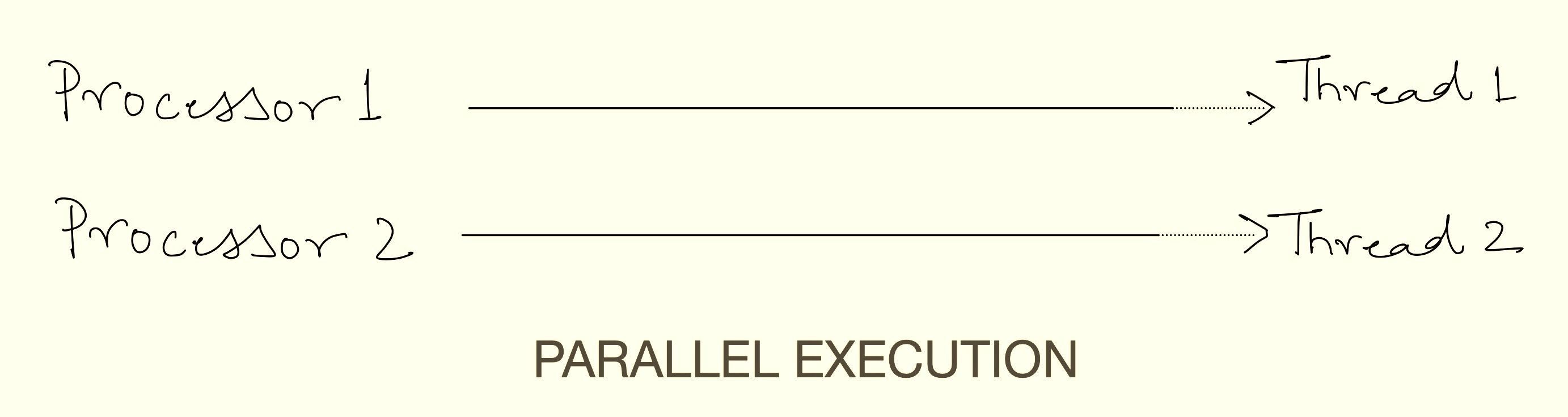
Parallel computing refers to the concept of executing two or more tasks or processes at the same time. On any general computing system, there are multiple different tasks running at the same time. For example, a browser running a video, a word processor for editing a document, the operating system, and so on. These tasks can be divided into separate and independent instruction streams known as “threads” which can be executed simultaneously. There are two ways of executing multiple threads, i.e., concurrency and parallelism. Parallel execution refers to executing multiple threads at the same time using multiple execution pipelines and concurrency refers to a single execution pipeline running multiple threads by switching between them without necessarily completing each one. A program can have either parallelism, concurrency, or a combination of the two. Individual physical execution pipelines on a processor are known as “cores”.

Superscalar Architecture: Single-core processors capable of concurrent execution of more than one thread are known as superscalar processors. A superscalar processor executes multiple instructions per clock cycle by dispatching them to different “execution units” within a single processor, unlike a scalar processor, which executes only one instruction per cycle. This increases instruction throughput beyond what a given clock rate alone allows. Each execution unit is not a separate processor or core but a resource within the processor (these are often referred to as “logical cores” as well). While superscalar processors are often pipelined, these are distinct techniques: superscalar execution runs multiple instructions in parallel across units, whereas pipelining splits a single execution unit into sequential phases for overlapping instruction execution.
SIMD (Single Instruction, Multiple Data): SIMD is a type of parallel processing where multiple processing elements perform the same operation on multiple data points simultaneously. This technique allows for efficient processing of large datasets, as it enables the execution of a single instruction on multiple data elements at once, thereby increasing computational throughput. SIMD is particularly useful for tasks that involve repetitive operations on arrays or vectors, such as adjusting the contrast in a digital image or performing complex mathematical computations. SIMD is part of Flynn’s Taxonomy of computer architectures ( other being single instruction stream, single data stream - SISD, multiple instruction streams, single data stream - MISD, multiple instruction streams, multiple data streams - MIMD).
Parallel computing techniques enable modern processors to handle complex workloads simultaneously with incredible speed, making them much more usable for general-purpose use in everyday life.
Multicore Processors: Doing More at Once
One of the most significant advances in scaling processor performance is the concept of multicore processors. Unlike, early single-core processors, which execute only a single instruction stream at a time, modern processors have multiple superscalar cores on a single chip. Each “core” operates independently as a processing unit with its own execution unit and instructions (or programs) to execute. Each core is superscalar and uses concurrent execution to exploit Task-Level Parallelism (TLP) which refers to the parallelism present in runtime environments and operating systems that execute multiple tasks simultaneously. This form of parallelism is predominantly observed in applications designed for commercial servers, such as databases. This combination of multiple superscalar cores on a single chip theoretically provides unlimited performance scaling, as long as you can keep packing more and more cores on the same chip. In practice, the complexities arising from managing the coherent execution of all the cores and physical constraints like power and area restrict multicore designs to scale efficiently past a few dozen cores. By running numerous threads concurrently, these applications can effectively manage the significant I/O and memory system latency associated with their workloads. While one thread is stalled waiting for memory or disk access, other threads can continue performing useful work, ensuring efficient resource utilisation.
Multicore processors shine in scenarios where tasks can be divided into smaller, independent chunks. Applications like video editing, 3D rendering, gaming, and scientific simulations benefit immensely from this architecture. However, not all software is designed to take advantage of multiple cores. Programs that rely on single-threaded execution—where tasks must be completed sequentially—may not see significant performance gains, even on high-end multicore processors. This is why some applications run faster than others on the same hardware, highlighting the importance of parallel programming in modern software development.
Caching: Speeding Up Data Access
The von Neumann architecture works on a stored-program concept. This means that for a processor to work efficiently, the instructions and data from computer’s memory must be fed at a rate that keeps up with the execution pipeline. Memory access is the limiting bottleneck of all high-performance processors (remember the von Neumann bottleneck) and hence modern processors are constantly evolving to mitigate the performance impact of it. One such mitigation is the architectural concept of “Memory Hierarchy”, an extension of which is “CPU Cache”. The memory hierarchy in a CPU is a system that organises different types of memory based on speed, size, and cost to ensure efficient data access. At the top, registers are the fastest but smallest, storing temporary values for immediate processing. Below them, cache memory (L1, L2, L3) is larger but slightly slower, storing frequently used data to reduce access time to main memory. The RAM (main memory) holds active programs and data but is much slower than the cache. At the bottom, storage (SSD/HDD) is the slowest and largest, used for long-term data storage, requiring significant time to access compared to other levels.
While Random Access Memory (RAM) is significantly faster than storage devices like SSDs, it’s still not fast enough to keep up with the blistering speed of modern CPUs. To bridge this gap, processors use cache memory, a small but ultra-fast type of memory located directly on the processor chip. A CPU cache is a small, high-speed memory within the processor designed to minimise the time required to access data from main memory. It stores copies of frequently used data, allowing quicker retrieval. Most CPUs feature a multi-level cache hierarchy (L1, L2, L3, and occasionally L4), with L1 typically divided into separate instruction and data caches. Cache memory is usually built using SRAM and occupies a significant portion of a modern processor’s chip area.
Cache memory is organised into hierarchical levels, each with its own size and speed trade-offs:
L1 Cache: The smallest and fastest cache, typically split into separate caches for instructions and data. It’s located closest to the CPU cores, offering near-instant access but limited storage capacity.
L2 Cache: Larger but slightly slower than L1, often shared between cores. It acts as a middle ground, balancing speed and capacity.
L3 Cache: The largest and slowest cache, shared across all cores. While slower than L1 and L2, it still provides a significant performance boost by reducing the need to access main memory.
Cache memory relies on the principle of “locality”, which observes that programs tend to access the same data or instructions repeatedly over short periods. This behavior is categorised into two forms: temporal locality (recently accessed data is likely to be accessed again soon) and spatial locality (data near recently accessed data is likely to be accessed next). By storing frequently used data in fast cache memory, the CPU reduces the need to fetch it from slower main memory, significantly speeding up execution. This principle is why even a small cache can dramatically improve performance—it ensures the CPU spends less time waiting and more time computing.
This hierarchical design ensures that the CPU spends less time waiting for data and more time executing instructions, making caches one of the most significant aspects of modern processor performance.
Mitigating the von Neumann Bottleneck
The von Neumann bottleneck—the limitation caused by the shared communication pathway between the CPU and memory—remains a challenge for modern processors. Although introducing memory hierarchy is extremely helpful, it is still not enough to scale processor performance to desired levels. With blazing-fast clock rates, modern processor cores are almost always faster than all the other components of a computer. This means that processors spend a sizeable portion of their time sitting idle and waiting for instructions to be executed. To extract every bit of performance from all the resources of a computer other architectural concepts are constantly being developed. Let’s look at some of the most widely used-
Branch Prediction: Branch prediction helps processors guess the outcome of a decision (branch) before it actually happens to avoid delays. When a program has an if-else statement or a loop, the processor predicts which path the program will take and starts executing instructions ahead of time. If the prediction is correct, execution continues smoothly; if it’s wrong, the processor discards the incorrect work and restarts from the right place. Advanced CPUs use machine learning-like techniques and past execution history to make better predictions. This reduces wasted time and improves performance.
Speculative Execution: Speculative execution allows a processor to execute instructions ahead of time, even before it knows for sure if they will be needed. It works together with branch prediction by assuming a predicted path and starting computations early. If the assumption is correct, the results are used immediately; if not, the incorrect work is discarded. This technique significantly improves speed by ensuring that the processor is always working on something useful instead of waiting. However, it has also led to security vulnerabilities like Spectre and Meltdown, which exploit how the processor temporarily stores speculative data.
Out-of-Order Execution: Out-of-order execution allows a processor to execute instructions out of their original program order to improve efficiency. Instead of waiting for one instruction to finish before starting the next, the processor looks ahead and finds other instructions that can be executed while waiting for slow operations like memory access. This helps keep the processor busy and reduces idle time. Once all instructions are completed, the processor reorders the results to match the original program sequence. This technique greatly improves performance, especially in modern high-speed processors.
Register Renaming: Register renaming helps solve conflicts when multiple instructions try to use the same CPU registers. Since there are only a limited number of registers, the CPU assigns hidden, extra registers to avoid unnecessary delays. This prevents one instruction from being stalled while another is still using a register. By renaming registers dynamically, the CPU avoids false dependencies and improves parallel execution. This is especially useful in out-of-order execution, where multiple instructions are processed at the same time.
Conclusion
Well, that’s it, we’ve now gone over every part of the computer that makes it compute (even if it is through gross oversimplification 🙂). From what a computer means to a user, what it computes, how humans instruct computers what to compute, and how computers understand those instructions and then execute them, each stage represents decades of engineering effort in dozens of different abstraction levels. These innovations have transformed computers from simple calculators into powerful machines capable of running complex applications such as artificial intelligence models, medical research, stock exchanges, weather simulations, and much more. Computers are arguably one of the most important inventions of entire human history, elevating the quality of life of billions of humans every day in ways unprecedented before. Processors are no less than a magical feat of the human mind. To think that we’ve taken sand, turned it into silicon, and then made it think is a testament to the ingenuity of our species.
Originally published on BitCrusader by Tanmay Goel (GuyPhy). Republished on Bluethroat Labs with the author's permission. Tanmay Goel has worked closely with Bluethroat Labs on multiple projects.
Footnotes
-
Compiled using -
Apple clang version 16.0.0 (clang-1600.0.26.6) Target: arm64-apple-darwin24.2.0 Thread model: posixusing command -
clang -S -o hello.s hello.c*Used an image instead of a code insert for syntax highlighting. ↩
-
Generated using -
Apple LLVM version 16.0.0 - ‘objdump’ utilityusing command -
clang -o hello hello.c | objdump -d hello↩ -
Generated using -
llvm-otool(1): Apple Inc. version cctools-1022.2 otool(1): Apple Inc. version cctools-1022.2 disassmbler: LLVM version 16.0.0and
'xxd' utility by 2024-09-15 by Juergen Weigert et al.using command -
otool -t hello | xxd -r -p | xxd -b↩